High power impulse magnetron sputtering (HiPIMS) is a growing technique promising high-quality film deposition for SRF/accelerator cavities. One of the basic requirements for Nb SRF coatings is the dense and void-free morphology. This is particularly challenging to be obtained in configurations with grazing angle of incidence of the impinging particles, which are therefore required to reach the substrate with higher energies to densify the growing film.
The highest power peak achieved during the pulsed plasma in HiPIMS allows ionizing the sputtered metal atoms. These ions can later on/then be accelerated towards the substrate by either biasing the substrate itself to a negative voltage, or by applying a positive voltage (positive pulse-PP) at the target during the afterglow. The PP approach provides some advantages, such as the simplified design of the magnetron, the use of a single power supply (or another way to say there is no need for a second one for biasing the substrate) and the possibility to keep the cavity at the ground voltage, which is critical for the coating of a SRF cavity that works also as vacuum chamber during the coating process. Ongoing R&D efforts are oriented towards the validation of the HiPIMS with PP technique in the framework of the FCC project, for the Wide-Open-Waveguide crab cavity. In a first step [1], the effective acceleration of the sputtered ions has been demonstrated for the first time by changing the duration of a 50V PP, observing a complete shift of the ion energy distribution function to values close to 30eV, as shown in Fig. 1.
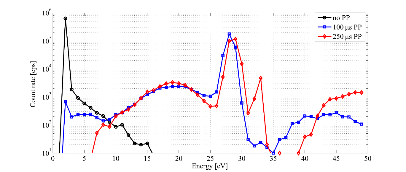
Fig 1: Time-integrated EDFs of Nb+ ions for the case without PP, +50 V PP of 100 μs, and 250 μs duration.
In a recent paper [2], the densification of coated Nb films on copper samples at 90deg angle of incidence was explored for different techniques, from the standard direct current magnetron sputtering (DCMS), to the HiPIMS with PP (Fig. 2).
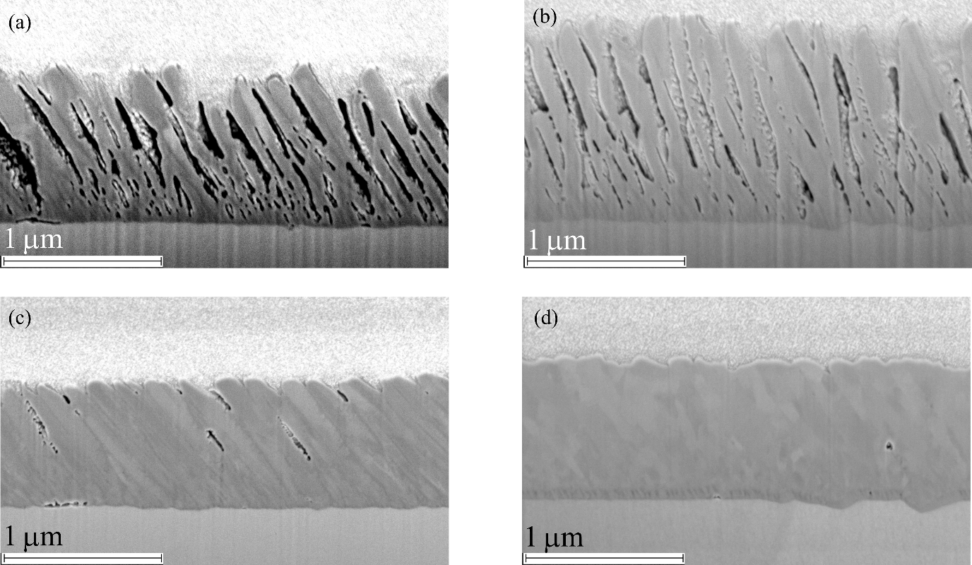
Fig 2: Nb films grown on copper substrate FIB cross sections of samples at 90∘ coated in: (a) DCMS with grounded substrate, (b) HiPIMS with grounded substrate, (c) HiPIMS with grounded substrate and +50 V PP, (d) HiPIMS with grounded substrate and +100 V PP.
A first step towards the validation of these coatings with respect to the SRF performances was also performed, by measuring the film critical temperature and the transition width in a dedicated test-stand at the CERN Central Cryogenic Laboratory, in the framework of the MSCA EASITrain project. An example of measured transition is depicted in Fig. 3.
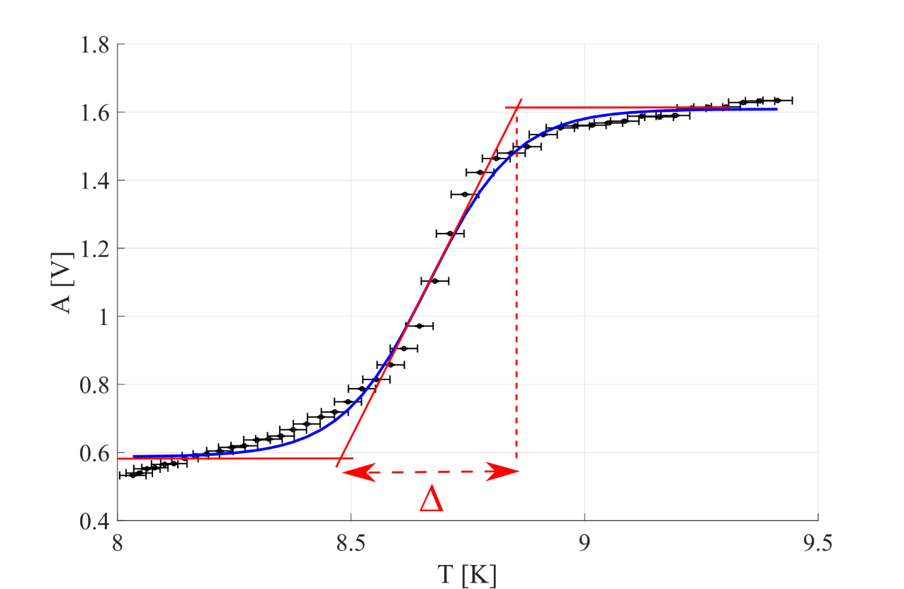
Fig 3: Coil measurement of the superconducting to normal conducting transition of grounded sample coated at 90∘ in HiPIMS with +100 V PP. The data points of the voltage amplitude of the pickup coil are shown in black with their error bars as a function of the average temperature. The data fit is displayed with a continuous blue curve. In red, the lines for the estimate of the transition width Δ.
A further validation on a quadrupole resonator sample has been performed providing residual resistance values comparable to those of bulk Nb. In the next months, the first coating of the full scale WOW cavity prototype will be performed in HiPIMS with PP.
Further reading:
[1] F Avino et al. 2019 Plasma Sources Sci. Technol. 28 01LT03. https://doi.org/10.1088/1361-6595/aaf5c9.
[2] F. Avino et al. Thin Solid Films 706 (2020) 138058. https://doi.org/10.1016/j.tsf.2020.138058.