Thin films have the potential to revolutionise superconducting radio frequency (SRF) cavities, which could in turn lead to massive cost savings for particle accelerators, allowing the groundbreaking sciences carried out by these facilities to not only continue, but to advance.
This is not new information, the scientific community involved in this area has known about this for over a decade and has been calling for support to carry out the necessary research to develop this technology.
But funding has been hard to come by, with the exception of certain EU projects, such as the current and ongoing I.FAST – Innovation Fostering in Accelerator Science and Technology, although even this is not enough.
Now, with material costs skyrocketing, the need for a solution in this area is becoming urgent, and yet the limited funding available is still only enough to cover the cost of a few first prototypes.
A slow start
There are several reasons why the development of specialised thin films for SRF has been slow.
One reason is that most developments in superconductors have been devoted to electromagnets under the impulsion of MRI developments -- medicine has always had more money than physics. A little-known fact is that SRF works in a different regime with different materials than electromagnets, meaning that developments in magnet technology do not necessarily benefit SRF.
Several thousands of superconductors have been identified since the discovery of superconductivity, but when it comes to applications only a dozen of them are used. They are all “type II”, which means they exhibit two different superconducting regimes: Meissner state at low field, where all magnetic flux is expelled from the material, and “mixed state” where some flux lines (so called vortices) penetrate the superconductor.
Electromagnets operate in the mixed state. To get very high current density, it is necessary to introduce defects to trap the vortices and prevent them from moving. This technology has benefited from the fact that realistic materials always exhibit plenty of defects, especially when one is at the development stage. Nowadays, defects are introduced on purpose in the material to reach very high current densities in magnets.
The development of SRF cavities started later. As they must operate in the Meissner state, materials optimised for magnet applications are not fit for SRF applications; they are even the worst-case scenario in terms of surface dissipations.
Niobium (Nb) is the material with the highest transition field between Meissner and mixed state, which explains why it is the material of choice for SRF. In RF, its dissipation is minimal: ~10⁵ orders of magnitude less than copper at the same frequency. But it presents some drawbacks: its price, which is now close to €1,000 per kilogram (more expensive than silver!), the fact that at high frequency it must operate at 2 K (high cryogenic costs), and finally, it is very close to its ultimate limits.
So, if one wants to bring SRF technology to higher performances – or the same performance with a drastic reduction of costs – one has to invent a new technology. It can only be based on thin films, which will be not only a way to overcome Nb’s comparatively low performance, but will also be a game changer in terms of energy consumption.
The thin film candidates
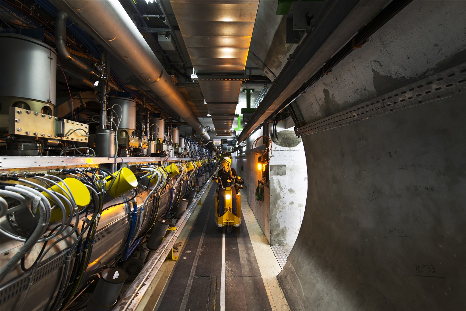
Since only a thin superconducting layer on the intern surface of a cavity is necessary, depositing a thin Nb layer into a copper cavity has been a potential solution for reducing costs for the past 50 years. Unfortunately, the crystalline quality of the Nb films is much less than the bulk material, and performance at high accelerating gradients is poor, keeping this application for circular accelerators and low accelerating gradients.
Many years of R&D have been invested in this solution, with some counterintuitive discoveries and many explored dead-ends. Only recently could one observe results closer to bulk performance on films. The key to success was a combination of more energetic deposition techniques on very clean copper and elimination of welding on the substrate.
Other solutions exist. On paper, one ideal superconductor is niobium–tin Nb³Sn, expected to reach accelerating gradients a factor of two times higher. Several cavities have been fabricated by thermal diffusion of Sn vapour inside Nb bulk cavities and they indeed exhibit very high Q₀ at 4.2 K. The ultimate field is still limited, with a behaviour indicating early field penetration at surface defects. There is an active R&D field to transpose these results onto copper cavities to reduce the fabrication cost of Nb³Sn cavities. The work on samples is fairly developed, but successful deposition inside cavities has not been reported yet.
Since the A15 materials – a class of intermetallic compounds known for their superconducting properties, of which Nb³Sn is one example – are so sensitive to the small composition variation, alternative materials like Niobium nitride (NbN) or niobium-titanium nitride NbTiN[1] have also been explored. They are much less sensitive than A15 to local composition, and their fabrication as thin film has been assessed for many years, since they are currently used in superconducting electronics.
The last explored material is Magnesium diboride (MgB²), which has the potential to be used at 10 K, opening the possibility to cool (small) cryomodules with cryocoolers, without the need of a large helium inventory. Promising work has been conducted on sample but deposition in a full RF cavity has never been conducted up to RF test.
The multilayers (SIS) concept: A possible revolution
A way to overcome this sensitivity to defects is to deposit Superconducting-Insulating-Superconducting (SIS) multilayers structures. They are metamaterials with very different properties from conventional superconductors.
As stated before, in RF the superconductors (SC) need to remain in the Meissner state, i.e. below the first critical field HC1. In fact, when the field is parallel to the surface (as in RF cavities), one can even reach a “superheating field” HSH> HC1, because flux lines must cross a surface barrier before entering the SC (figure 1-a).
In the presence of defects (inclusion, sharp feature…) the surface barrier disappears, and vortices start to enter in avalanche, causing early transition of the SC (Figure 1-b). By inserting a dielectric layer a few 10s of nm under the surface layer, one can block the propagation of vortices (figure 1-c) and consequently enhance the possible accelerating gradient (which is proportional to the magnetic field inside the cavity). Finally, if one uses a higher critical temperature (T꜀) SC as a top layer one can also decrease surface resistance and operate at higher temperatures (figure 1-d).
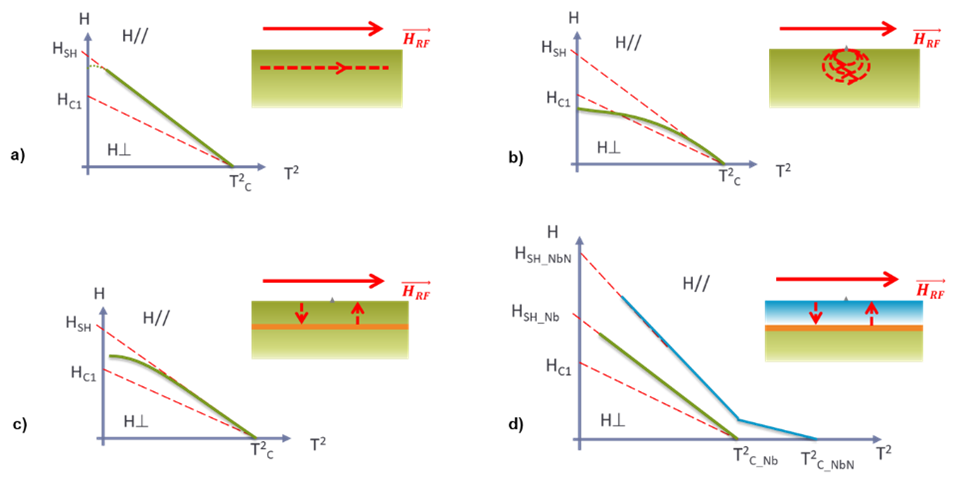
With multilayers, one can both gain on the quality factor and the accelerating field. This structure is much less sensitive to the presence of defects, which are always present when fabricating complex materials. It might be the only way to produce the advanced materials mentioned earlier at large scale, with a significant yield.
Very recently, it has been calculated that the use of pnictides[2] in the form of SIS multilayers could provide desirable performances at liquid nitrogen temperature (plug power divided by 25!)[3]. If this development can be financed and works, it could lead to a revolution in SRF technology.
European activities
The next generation of SRF technology presents huge challenges in material science, with a very vast number of parameters to be explored. This kind of R&D has been poorly[4] supported over the years, but a series of European projects, I.FAST the latest one, have helped to federate European activities in this domain.
The best solution will not necessarily exhibit the best superconducting performances, it will rather be a compromise between high superconducting and RF performance, easy fabrication process, high reproducibility at “industrial scale”, having an easy process to go from 1-cell to multi-cells or complex shapes, an easy process to adapt to various frequencies, tunability (many of the high Tc superconductors are brittle), low sensitivity to trapped flux upon cooling down, few crystalline defects or a structure not too sensitive to them (e.g. SIS structures)…
It also requires the development of mandatory aspects: fabrication and surface preparation of the copper substrates, the development of new cooling schemes (e.g. with cryocoolers), the development of specific characterisation tools since classical techniques are still not able to be predictive in terms of surface resistance.
Now that the R&D community is at the eve of depositing the first prototypes, access to SRF testing hardware (surface preparation, cleanrooms, RF test stands…) will be needed at a larger scale, and will probably soon become a bottleneck. Coordination between labs is more than ever a necessity. One of the main outcomes of the I.FAST project’s work package 9 on thin films will be the writing of a R&D European roadmap, established in collaboration with other international labs, and that will pave the way for needed coordinated R&D after 2025.
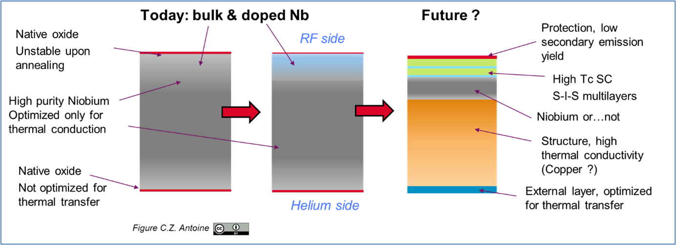
The future of SRF lies within a fully tailored multi-layered material where each layer is taking care of a given objective: thermal transfer, diffusion or protection barrier, high performance superconductivity, low secondary emission yield (protection against multipacting)… as depicted in figure 2.
Thin superconducting films are liable to lead to appreciable cost savings in accelerator technology, from the investment point of view as well as operation costs. Only RF tests of several prototypes will allow us to determine the best material since several requirements need to be met, mainly RF, superconducting properties but also fabrication ease and yield, tunability, etc.
Substantial support is needed if one wishes to apply this technology in the near future.
- The presence of Ti just helps to stabilize the correct crystalline phase in NbN.
- Recently found high Tc materials based on Fe and As.
- A. Mysazaki, TTC meeting 2023
- Investments in material science for RF application are far behind what has been done in the 70-80s for magnet development, with the consequence that TRL of these developments are still low and far from all the possible identified industrial applications.